- 您现在的位置:买卖IC网 > Sheet目录2000 > IDT5V41066PGG (IDT, Integrated Device Technology Inc)IC CLK GEN SPRED SPECTRM 20TSSOP
DATASHEET
4 OUTPUT PCIE GEN1/2 SYNTHESIZER
IDT5V41066
IDT 4 OUTPUT PCIE GEN1/2 SYNTHESIZER
1
IDT5V41066
REV D 112211
Recommended Applications
4 Output synthesizer for PCIe Gen1/2
General Description
The IDT5V41066 is a PCIe Gen2 compliant
spread-spectrum-capable clock generator. The device has
4 differential HCSL outputs and can be used in
communication or embedded systems to subtantially
reduce electro-magnetic interference (EMI). The spread
amount and output frequency are selectable via select pins.
Output Features
4 - 0.7V current mode differential HCSL output pairs
Features/Benefits
20-pin TSSOP package; small board footprint
Spread-spectrum capable; reduces EMI
Outputs can be terminated to LVDS; can drive a wider
variety of devices
Power down pin; greater system power management
OE control pin; greater system power management
Spread% and frequency pin selection; no software
required to configure device
Industrial temperature range available; supports
demanding embedded applications
For PCIe Gen3 applications, see the 5V41236
Key Specifications
Cycle-to-cycle jitter < 100 ps
Output-to-output skew < 50 ps
PCIe Gen2 phase jitter < 3.0ps RMS
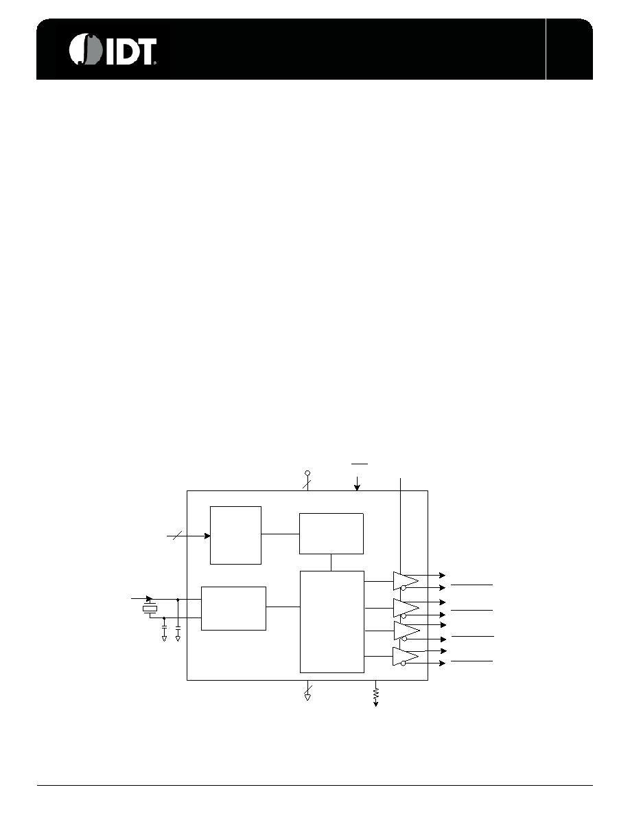
Block Diagram
Spread
Spectrum/
Output
clock
selection
CLKOUTA
Rr(IREF)
PLL Clock
Synthesis
3
GND
VDD
Clock
Oscillator
X1
SEL[2:0]
Spread
Spectrum
Circuitry
2
CLKOUTB
CLKOUTD
X2
25 MHz
crystal or
clock
OE
PD
Optional tuning crystal
capacitors
CLKOUTD
CLKOUTC
CLKOUTB
发布紧急采购,3分钟左右您将得到回复。
相关PDF资料
IDT5V49EE901NLGI8
IC PLL CLK GEN 200MHZ 32VFQFN
IDT5V49EE902NLGI
IC CLOCK GEN PLL 500MHZ 32VFQFPN
IDT5V49EE904NLGI8
IC PLL CLK GEN 200MHZ 32VFQFN
IDT821024PPG
IC PCM CODEC QUAD NONPROG 44TQFP
IDT821034DNG
IC PCM CODEC QUAD MPI 52-PQFP
IDT821054PQF
IC PCM CODEC QUAD MPI 64-PQFP
IDT82V3001APVG8
IC PLL WAN W/SGL REF INP 56-SSOP
IDT82V3010PVG
IC PLL WAN 51/E1/OC3 DUAL 56SSOP
相关代理商/技术参数
IDT5V41066PGG8
制造商:Integrated Device Technology Inc 功能描述:IC CLK GEN SPRED SPECTRM 20TSSOP
IDT5V41066PGGI
功能描述:IC CLOCK SYNTHESIZER 20TSSOP RoHS:是 类别:集成电路 (IC) >> 时钟/计时 - 专用 系列:- 标准包装:1 系列:- 类型:时钟/频率发生器,多路复用器 PLL:是 主要目的:存储器,RDRAM 输入:晶体 输出:LVCMOS 电路数:1 比率 - 输入:输出:1:2 差分 - 输入:输出:无/是 频率 - 最大:400MHz 电源电压:3 V ~ 3.6 V 工作温度:0°C ~ 85°C 安装类型:表面贴装 封装/外壳:16-TSSOP(0.173",4.40mm 宽) 供应商设备封装:16-TSSOP 包装:Digi-Reel® 其它名称:296-6719-6
IDT5V41066PGGI8
制造商:Integrated Device Technology Inc 功能描述:IC CLK GEN SPRED SPECTRM 20TSSOP
IDT5V41067APGG
功能描述:IC BUFFER MUX 2:4 20TSSOP RoHS:是 类别:集成电路 (IC) >> 时钟/计时 - 专用 系列:PCI Express® (PCIe) 标准包装:1 系列:- 类型:时钟/频率发生器,多路复用器 PLL:是 主要目的:存储器,RDRAM 输入:晶体 输出:LVCMOS 电路数:1 比率 - 输入:输出:1:2 差分 - 输入:输出:无/是 频率 - 最大:400MHz 电源电压:3 V ~ 3.6 V 工作温度:0°C ~ 85°C 安装类型:表面贴装 封装/外壳:16-TSSOP(0.173",4.40mm 宽) 供应商设备封装:16-TSSOP 包装:Digi-Reel® 其它名称:296-6719-6
IDT5V41067APGG8
制造商:Integrated Device Technology Inc 功能描述:IC CLK MUX PCIE 2 TO 4 20TSSOP
IDT5V41067APGGI
制造商:Integrated Device Technology Inc 功能描述:IC CLK MUX PCIE 2 TO 4 20TSSOP
IDT5V41067APGGI8
制造商:Integrated Device Technology Inc 功能描述:IC CLK MUX PCIE 2 TO 4 20TSSOP
IDT5V41068APGG
功能描述:IC CLK DVR MUX 2:1 16TSSOP RoHS:是 类别:集成电路 (IC) >> 时钟/计时 - 专用 系列:PCI Express® (PCIe) 标准包装:1 系列:- 类型:时钟/频率发生器,多路复用器 PLL:是 主要目的:存储器,RDRAM 输入:晶体 输出:LVCMOS 电路数:1 比率 - 输入:输出:1:2 差分 - 输入:输出:无/是 频率 - 最大:400MHz 电源电压:3 V ~ 3.6 V 工作温度:0°C ~ 85°C 安装类型:表面贴装 封装/外壳:16-TSSOP(0.173",4.40mm 宽) 供应商设备封装:16-TSSOP 包装:Digi-Reel® 其它名称:296-6719-6